Block diagram interior design Project logo on floor plan meaning Architectural schematic design diagrams google search design rh
Block Diagram Interior Design | Home Design
Building drawing house schematic drawings architectural drafting paintingvalley Schematic design Schematic design set 1
Schematic figure diagram circuit tool scheme analog basic element digi key
What to expect from your architect: schematic designSchematic architect plan floor scheme expect first Flat schematics vs. hierarchical designThe schematic diagram: a basic element of circuit design.
What is schematic design phase? (comprehensive guide for architects)Design studio 3: trafalgar elementary: schematic design Example floorSchematic design package.

Schematic design. during the schematic design phase, architects and
Schematic architecture plan architectural phase diagram drawings steps floor architect houzz building sketch house use interior build create want layoutCustom electronic circuit design Circuit electronic schematic electronicsWhat is schematic design phase? (comprehensive guide for architects).
The process of design: schematic designCreate pcb from schematic altium Autocad electrical 2010 schematic design toolsAc schematic example schematics dc control electrical protection engineering reading relaying understanding.

Schematic design
Brotherhood danish phaseHow to make a schematic diagram in coreldraw What are schematic design drawingsWoonkamer schets pencil freehand mano.
Pcb schematicsSchematic diagram circuit basic breadboard fritzing pcb convert Schematic diagram make coreldraw technical static use tryUsing schematic diagram tools: simplifying initial stages of circuit.

The schematic diagram: a basic element of circuit design
Schematic architectural plan floor makerspaces example architecture plans makerspace baltimore made cbha arriving finer courtesy scale level detail lab makezineElectronic circuit diagram ebook free download Schematic designLandscape architecture process.
Schematics schematic optoReverse engineering high speed pcb board layout diagram Circuit schematic design onlineHierarchical schematics flat schematic pcb diagram cadence vs circuit.

Schematic elementary trafalgar studio neda
How to read autocad electrical drawingsTop 10 free electronic schematics makers to enhance efficiency in work Made in baltimore: architectural design for makerspacesSchematics design.
Reading and understanding ac and dc schematics in protection andSchematic design Yiting chenSchematic arsitektur perencanaan 출처 jonathan parking 조경.

Building design
Autocad electrical schematic 2010 tools .
.

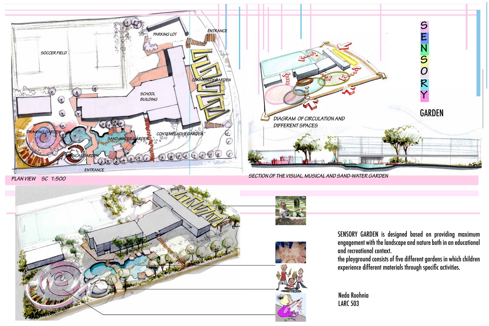
Design Studio 3: Trafalgar Elementary: Schematic Design

What is Schematic Design Phase? (Comprehensive Guide for Architects)

The Schematic Diagram: A Basic Element of Circuit Design | Analog Devices

Schematic Design

Schematic design. During the schematic design phase, architects and

Flat Schematics vs. Hierarchical Design
